Micro Star Technology
Diamond Instruments for Microscopy and Nano Technology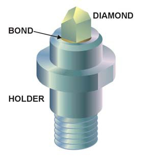
NANO INDENTERS
Micro Star makes a variety of nano indenters following defined standards. They also make custom requested geometries with customer-defined dimensions.
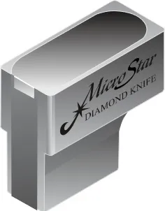
DIAMOND KNIVES
Micro Star makes seven different styles of diamond knives from carefully selected natural diamonds. Each of these can be mounted into five different boat styles.
DIAMOND AND OTHER MATERIALS
Diamond is the primary material for nano indentation. Only single crystal diamond, free of impurities or inclusions is used. Most Micro Star diamond nano indenters are shaped at one end of a large square section prism, as seen on some of the illustrations.
Diamond indenters are accurately aligned with the atomic crystal orientation such that the axis is in line with the 100 directions. One face of 3-sided and all four faces of 4-sided indenters follow the 100 crystal direction. Other crystal orientations are available at customer request.
DIAMOND KNIFE EXCHANGE & RESHARPENING
Exchange any Brand – All types of diamond knives from any manufacturer (including Micro Star), of any age or size, are accepted in exchange for a new Micro Star diamond knife. If we can resharpen the diamond knife as is, we charge the resharpen price. If the diamond is badly damaged or the knife cannot otherwise be resharpened, it will be replaced at our exchange price.
Resharpening Service – Regardless of the age or size, most diamond knifes are accepted for resharpening, if the diamond is not damaged beyond repair. It will be refurbished to the same Micro Star guaranteed flawless quality and the same angle and size of your original knife. If these standards cannot be met, a new diamond will be sent at no extra cost.
Need Consulting or a Quotation?
Contact Us Today! We are here to help.
Indenter Quote?
Diamond Knife Quote?
Knife Exchange Service?
Micro Star Technology
511 FM 3179 Road
Huntsville, TX 77340
Tel: 936 291 6891